Test Index
CBSE Class 12 Physics 2013 Paper
© examsnet.com
Question : 27 of 29
Marks:
+1,
-0
(a) Why is the base region of a transistor thin and lightly doped ? (b) Draw the circuit diagram for studying the characteristics of an transistor in common emitter configuration. Sketch the typical (i) input and (ii) output characteristics in this configuration. (c) Describe briefly how the output characteristics can be used to obtain the current gain in the transistor. OR(a) How is a depletion region formed in - junction?(b) With the help of a labelled circuit diagram, explain how a junction diode is used as a full wave rectifier. Draw its input, output wave-forms.(c) How do you obtain steady d.c. output from the pulsating voltage?
Solution:
Ans. OR (a) Formation of depletion region: When type and type semiconductors are brought in contact, electrons diffuse from -side to -side and holes diffuse from -side to -side. This is due to the higher concentration of holes in -side and higher electron concentration in -side. The electrons and holes cross the junction and recombine with each other. Thus a certain region of both side of the actual junction becomes depleted from free charge carriers. There remain only immobile positive ions in -side and immobile negative ions in -side which restrict further electrons and holes to cross the junction. Thus a depletion region is formed. (b) Full wave rectifier: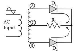 A full wave rectifier is constructed using two junction diodes, a centre-trapped transformer and a load resistor. Anodes of the diodes are connected at the two end terminals of the secondary of the transformer. Cathodes of the diodes are joined together and connected to the centre tap of the transformer through the load resistor. is fed to the input of the transformer. For the positive half cycle of is is 0 and is . So, is forward biased and is reverse biased. Current flows only through in the direction as shown. For the negative half cycle of is is 0 and is . So, is forward biased and is reverse biased. Current flows only through in the direction as shown. So, in both the cases, the direction of current through load resistor is in the same direction. So, a direct potential difference i.e., DC voltage is developed across the resistor . Input Output waveform:
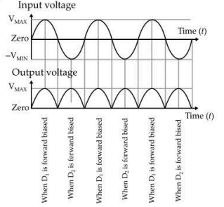 (c) To obtain steady DC output from the pulsating voltage, filter is to be used. Capacitor in parallel is an effective filter.
© examsnet.com
Go to Question: